webmaster

A highly detailed, professional macro photograph of a state-of-the-art semiconductor chip wafer, showcasing intricate nanometer-scale circuitry patterns and microscopic transistors. The wafer is bathed in a soft, futuristic light, reflecting advanced lithography processes. In the background, out of focus, subtle elements suggest a cleanroom environment with robotic precision tools or AI-driven optical inspection systems. The image emphasizes innovation and technological advancement. safe for work, appropriate content, fully clothed, professional, perfect anatomy, correct proportions, well-formed hands, proper finger count, natural body proportions.

Diseño de semiconductores Los casos que transformarán tu visión y te harán ganar

webmaster

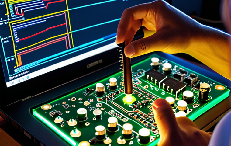
Cuando uno se adentra en el vertiginoso universo del diseño de semiconductores, es imposible no sentir una mezcla de asombro ...

**Circuit analysis learning**: A close-up shot of someone studying a circuit board with resistors, capacitors, and inductors, illuminated by the glow of a SPICE simulation software on a laptop in the background.

Electrónica: Secretos para Dominar las Asignaturas Clave y No Perder Dinero.

webmaster

Estudiar ingeniería electrónica es como adentrarse en un universo fascinante donde la electricidad, los circuitos y los microchips cobran vida. ...